

Ensure peak performance with advanced KGD testing solutions
In the relentless drive towards smaller, faster, and more powerful semiconductors, process optimization is a strategic imperative.
Known Good Die (KGD) testing is a critical linchpin in achieving manufacturing excellence. By meticulously vetting the functionality of each die before the investment of packaging, KGD provides a powerful lever for maximizing yield, minimizing waste, and controlling costs. It’s a proactive approach that eliminates the downstream impact of faulty die, ensuring that only viable components advance through the production pipeline, paving the way for superior product reliability and a competitive edge.
ipTEST, a member of the Microtest Group, leads the field in advanced KGD testing techniques for power device manufacturing. With decades of experience and cutting-edge technology, ipTEST delivers precise, reliable testing systems that support a wide range of technologies, including SiC, GaN, MOSFETs, and IGBTs, enabling manufacturers to achieve new quality and performance standards.
Explore advanced methods for Known Good Die (KGD) testing
Combining cutting-edge technology with unmatched precision, our offerings enable manufacturers to evaluate a wide variety of device types, ranging from conventional IGBTs and MOSFETs to advanced SiC and GaN devices, while achieving the highest standards of efficiency and performance.
In high-stakes applications such as automotive multi-chip modules, where 36+ individual die may be integrated into a single module, ensuring high yield rates is critical. To maintain economic viability, a module yield of at least 85% requires an average die yield of 99.55%, assuming a defect-free assembly process.
Achieving such stringent quality levels demands more than just basic wafer-level parametric screening. Subtle defects that might not surface during standard tests could still compromise the final product, necessitating advanced testing methodologies that extend beyond wafer-level evaluation to include individual die screening after dicing.
ipTEST offers industry-leading innovations for KGD testing, providing precise and thorough analysis to identify and eliminate defects at the earliest possible stages. These systems are designed to maximize yield while minimizing waste, supporting the growing demand for high-quality dies in applications such as automotive, industrial, and energy sectors.
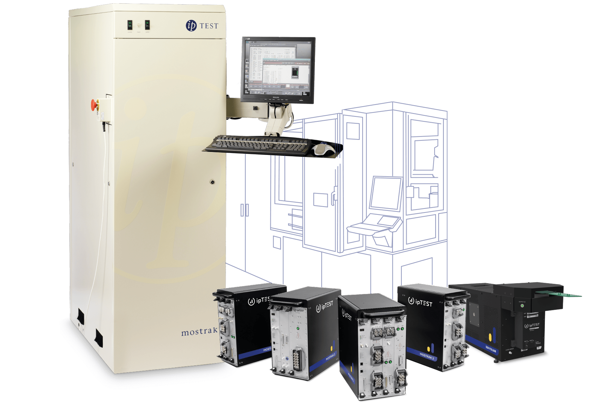
ipTEST MOSTRAK 2: Redefining KGD Testing

MOSTRAK 2 represents a new generation of KGD testers, combining cutting-edge technology with a focus on flexibility and precision. Designed to handle the demands of modern semiconductor production, this advanced product delivers unmatched performance and adaptability for a variety of production environments.
Key features of the MOSTRAK 2 product range includes:
MOSTRAK 2 enhances throughput by testing multiple dies simultaneously, significantly reducing overall testing time while maintaining accuracy and increasing production efficiency.
the method captures and evaluates high-speed switching waveforms, identifying subtle anomalies that standard tests might miss. Precision measurement algorithms ensure accurate and repeatable results, logging defects that could impact real-world performance while minimizing false rejects and enhancing yield.
incorporating the latest techniques to simulate real-world operational conditions, MOSTRAK 2 evaluates each die’s performance and stress tolerance over a range of temperatures (subject to handler/prober capabilities), verifying its ability to meet industry standards for reliability and durability.
flexible hardware and software interfaces allow compatibility with a wide range of wafer probers, handlers, and production workflows, ensuring easy adoption into existing manufacturing lines.
MOSTRAK 2 is adaptable to a wide range of production needs, from small-scale operations to high-volume manufacturing, providing an ideal solution for manufacturers at any stage of growth.
incorporates specialized hardware and software tailored for static, dynamic, thermal, and stress testing.
safeguards the tester and contactor from potential damage caused by device faults, reducing downtime and ensuring reliable testing performance.
Comprehensive testing ensures long-term reliability, reducing the risk of field failures and costly warranty claims. Additionally, high-throughput testing capabilities enable faster time-to-market, giving manufacturers a competitive edge in today’s rapidly developing semiconductor industry.
As semiconductor technologies continue to evolve, ipTEST systems remain adaptable, supporting emerging device topologies and evolving production needs.
 technology for KGD test safety
When KGD devices fail, a significant amount of current flows through the die (and tester + contactor) and a safety mechanism needs to be in place. That’s why we’ve integrated cutting-edge overcurrent protection (OCP) mechanisms into our dynamic switch test stations.
SocketSafe™ acts as a safety net, swiftly detecting, limiting, and diverting energy surges when faults occur during Known Good Die (KGD) tests. By capping energy transfer to a safe maximum, this innovative circuitry not only protects valuable testing equipment but also ensures that faulty devices dissipate energy safely and efficiently.
This proactive approach minimizes the need for contactor repairs, reduces costly downtime, and extends the lifespan of testing systems.
With SocketSafe™, manufacturers achieve optimal uptime and Unit Per Hour (UPH) rates. ipTEST’s precision-engineered solutions ensure unmatched safety and reliability, supporting your drive toward production excellence. Protect your investment, maintain peak performance, and stay ahead in a competitive market with Microtest’s Group’s advanced OCP technologies.
The critical role of KGD testing in semiconductor manufacturing
Known Good Die (KGD) testing plays a pivotal role in ensuring the reliability and performance of individual die, particularly in the production of high-performance devices such as Silicon Carbide (SiC). By identifying defective die early in the manufacturing process, KGD testing minimizes the risk of costly downstream failures and enhances overall product quality.
KGD testing acts as a vital quality checkpoint, ensuring that only functional and reliable die progress to the final stages of production.

Early detection of defects through KGD testing reduces waste, lowers manufacturing costs, and accelerates time-to-market. It enables manufacturers to focus resources on building products with proven reliability, strengthening customer trust and providing competitive advantage.
With advanced configurations designed to address the unique challenges of next-generation power devices, we empower manufacturers to achieve superior quality and operational efficiency. By investing in robust KGD testing solutions, companies can confidently meet the demands of today’s technology-driven world.
Comprehensive testing for different device types
The semiconductor industry develops a wide variety of power devices, each with distinct specifications and challenges. Comprehensive testing is crucial to verify that every die meets performance standards before being incorporated into packages or larger models.
Advanced testing platforms enable extensive coverage across various device types, giving manufacturers the flexibility to evaluate multiple technologies using a single, unified system.
Repeatable testing capabilities are essential for manufacturers striving to achieve standardized quality across large production batches. Consistent results play a crucial role in maintaining customer confidence and complying with stringent Gauge reliability and repeatability requirements.
High accuracy and robust reliability form the foundation for maximizing yield and ensuring success in the competitive semiconductor industry.
Identifying defects at the start of the production process plays a vital role in ensuring high yields and lowering costs. Advanced KGD-level testing uncovers even subtle issues before components move to next steps. This method prevents defective dies from advancing, preserving valuable resources and improving overall production efficiency. By addressing faults early, manufacturers can maintain higher yields and reduce material waste.
Reliability and performance are fundamental for industries like automotive, aerospace, and industrial automation. Each die undergoes rigorous evaluation to confirm compliance with the highest quality standards, significantly reducing the chance of failures in the field. Removing flawed components during initial testing enhances product reliability, fosters customer trust, and minimizes expenses linked to returns and warranty claims, ultimately bolstering the brand’s reputation.
Overlooked defects in the manufacturing process increase costs, particularly during packaging and assembly. KGD testing allows manufacturers to filter out defective dies early, avoiding unnecessary expenses and reducing material waste. This approach ensures a more efficient use of resources and eliminates the need for costly rework or retesting, streamlining production and lowering operational costs across the board.
Fast production cycles are crucial in the competitive semiconductor landscape. High-throughput testing models evaluate multiple dies simultaneously, eliminating bottlenecks and enabling quicker product delivery. With scalability designed to accommodate future technologies like SiC and GaN, these methods ensure manufacturers remain agile and competitive. Faster testing and seamless integration into production lines support accelerated time-to-market without compromising quality.
Why choose Microtest Group for KGD testing needs?
Selecting an experienced and capable partner for Known Good Die (KGD) testing is essential for maintaining the efficiency and reliability of semiconductor manufacturing processes.
Advanced technology for high-performance testing
Microtest Group’s ipTEST equipment are designed with cutting-edge technology to address the complexities of modern semiconductor manufacturing. Featuring advanced instrumentation and robust algorithms, these innovative approaches provide thorough diagnostic capabilities for a wide variety of devices, including MOSFETs, IGBTs, SiC, and GaN components.
Microtest operates globally within the semiconductor ecosystem with 2 areas of expertise: ATE (Automatic Test Equipment) and Advanced ASIC Services.
- Save Space
- Reduce the Total Cost of Ownership
- Save Power consumption
- Reduce Time-to-market
The Microtest Group operates in the semiconductor ecosystem, providing best-in-class ate, test services, and asic design for the automotive, industrial, power, sensor and healthcare markets.
experience
worldwide